|
|
|
|
|
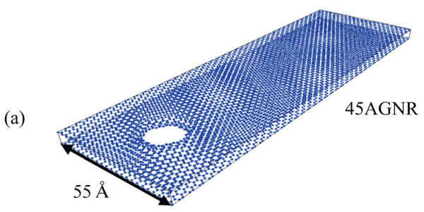
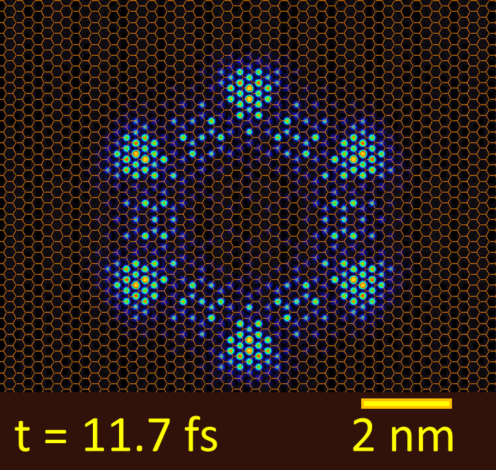
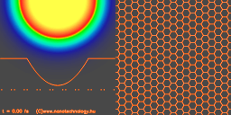
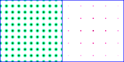
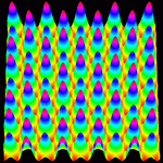
How does a hole influence electronic conduction of a bilayer graphene nanoribbon?
|
|
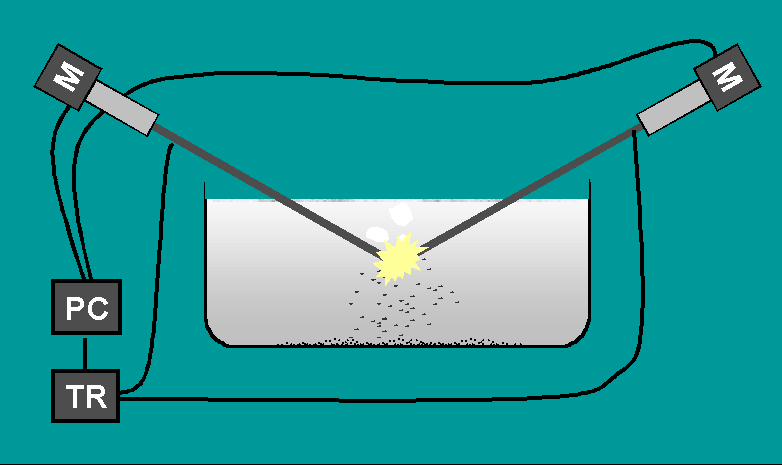
Wave packet dynamics makes us possible to calculate the transport of electrons in nanosystems containing
several thousands of atoms.
Figure (a) shows the atomic structure of a bilayer graphene nanoribbon, where the two layers are connected
along the cicumference of a hole.
Figure (b) and (c) show two electrode configarations used in our calculations.
We found that the hole is a kind of energy filter, by changing the voltage applied across the electrodes,
it is possible to control the transmission, delay, and reflection of the wave packet.
|
Publication
>>
|
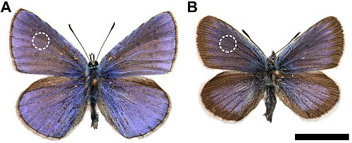
Reproducible phenotype alteration due to
cooling of the pupae of
butterflies
 |
|
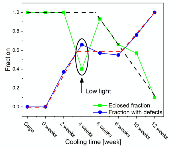
Understanding the causal links between the genotype of an organism, the environmental factors, and its
phenotype is a hot topic in current biology.
We investigated in detail, how an environmental factor (prolonged cooling of the pupae)
influence the wing structure of the adult butterflies.
This graph shows, that a relatively short cooling (up to 2 weeks) does not influence
the eclosed fraction, but somewhat increases the number of wing defets.
A prolonged cooling (more that 10 weeks), however, decreases the eclosed fraction to zero.
Good illumination during pupation is also an essential factor (see the point marked "low light").
|
Publication
>>
|
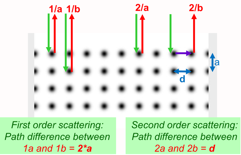
First- and second order light scattering processes in biological photonic nanostructures
 |
|
The image shows a real space lattice of four translation periodic layers
with lateral periodicity d and layer distance a.
The arrows show the possible light scattering processes -- green is the incoming light,
red is the outgoing light.
The first- and second order processes (left and right, respectively) give spectral peaks
at different locations.
In this work we showed that for butterfly wings the visible part of the spectum is generally
well reproduced by taking into account first order scattering only, but the second
order contribution is important at the UV range.
|
Publication>>
|
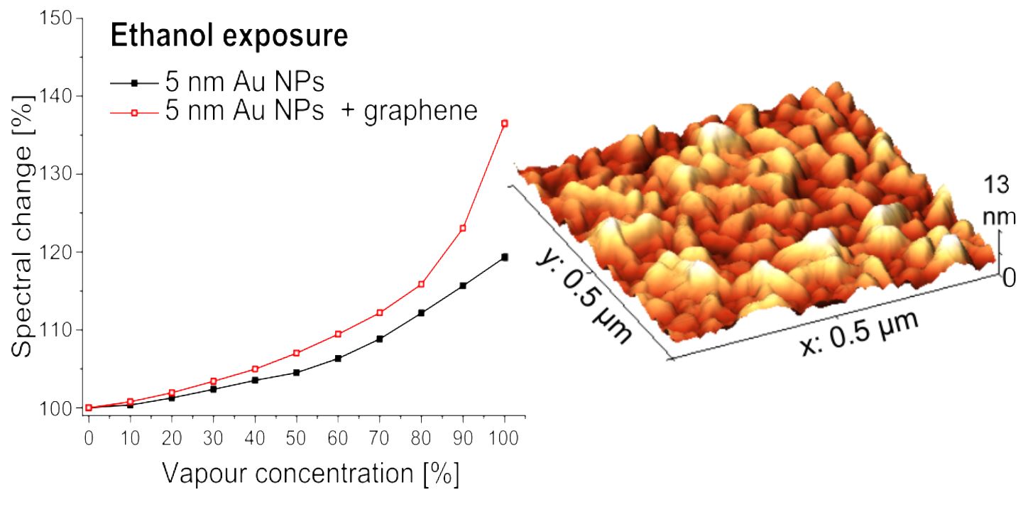
Vapour sensing properties of graphene-covered gold nanoparticles
 |
|
We investigated the vapour sensing properties of different graphene-gold hybrid nanostructures. We observed the shifts in the optical spectra near the local surface plasmon resonance of the gold nanoparticles by changing the concentration and nature of the analytes (ethanol, 2-propanol, and toluene). The smaller, dome-like gold nanoparticles proved to be more sensitive to these vapours compared to slightly larger, flat nanoparticles. We investigated how the optical response of the gold
nanoparticles can be tuned with a corrugated graphene overlayer. We showed that the presence of rippled graphene increased the sensitivity to ethanol and 2-propanol, while it decreased it towards toluene exposure (at concentrations higher than 30%). The slope changes observed on the optical response curves were well described by capillary condensation. These results can have potential impact on the development of sensors based on graphene gold nanohybrids.
|
Publication>>
|
Dynamic strain in gold nanoparticle supported graphene induced by focused laser irradiation
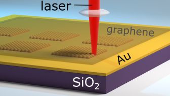 Graphene on noble-metal nanostructures constitutes an attractive nanocomposite with possible applications in sensors or energy conversion. In this work we study the properties of hybrid graphene/gold nanoparticle structures by Raman spectroscopy and scanning probe methods. The nanoparticles (NPs) were prepared by local annealing of gold thin films using a focused laser beam. Graphene grown by chemical vapour deposition was transferred onto the prepared, closely spaced gold NPs.
We found that laser irradiation (and the associated high temperature) induced a dynamic hydrostatic strain in graphene on Au NPs, which turned out to be completely reversible. These results can have implications in enhancing the sensing properties of graphene/plasmonic nanoparticle hybrids using strained graphene in high temperature regime. .
Graphene on noble-metal nanostructures constitutes an attractive nanocomposite with possible applications in sensors or energy conversion. In this work we study the properties of hybrid graphene/gold nanoparticle structures by Raman spectroscopy and scanning probe methods. The nanoparticles (NPs) were prepared by local annealing of gold thin films using a focused laser beam. Graphene grown by chemical vapour deposition was transferred onto the prepared, closely spaced gold NPs.
We found that laser irradiation (and the associated high temperature) induced a dynamic hydrostatic strain in graphene on Au NPs, which turned out to be completely reversible. These results can have implications in enhancing the sensing properties of graphene/plasmonic nanoparticle hybrids using strained graphene in high temperature regime. .
|
Publication>>
|
Simulation of vapor dependent spectra of butterfly wings
 The reflection spectrum of butterfly wings shows small, but selective changes when subjected to vapors of different liquids.
We measued and modeled this phenomenon on such an exceptional butterfly species, Albulina metallica, where the colors of both the upper and lower wing surfaces are
physical colors, i.e. given by photonic nanoarchitectures.
Figure (a) shows a cross sectional transmission electron micrograph (TEM) of a wing scale of a male Albulina metallica. The dark areas are chitin and the light holes are air voids in the chitin.
Figure (b) is the model structure we used in our calculation.
Measured and calculated spectra match well.
.
The reflection spectrum of butterfly wings shows small, but selective changes when subjected to vapors of different liquids.
We measued and modeled this phenomenon on such an exceptional butterfly species, Albulina metallica, where the colors of both the upper and lower wing surfaces are
physical colors, i.e. given by photonic nanoarchitectures.
Figure (a) shows a cross sectional transmission electron micrograph (TEM) of a wing scale of a male Albulina metallica. The dark areas are chitin and the light holes are air voids in the chitin.
Figure (b) is the model structure we used in our calculation.
Measured and calculated spectra match well.
.
|
Publication -- measurement
>>
Publication -- simulation
>>
Video abstract (EN)
>>
Video abstract (HU)
>>
|
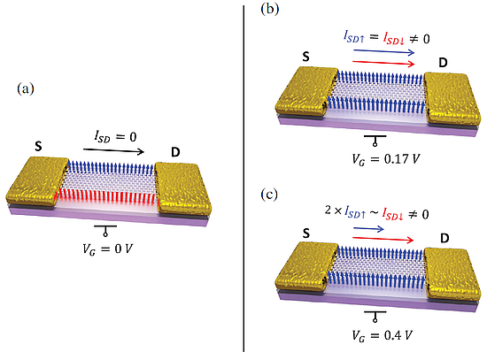
Three-state graphene transistor for electronics and spintronics
 |
|
This image shows the three states of a graphene transistor made of a graphene nanoribbon.
According to our theoretical calculations, this transistor has three separate magnetic
states, tunable merely with a back gate electrode, without the need of ferromagnetic contacts.
This device can serve as a basic building block of hybrid electronic and spintronic graphene
data processing systems.
|
Publication
>>
|
Changes in structural and pigmentary colours in response to cold stress in butterflies
 |
|
During the past decade, the color patterns of insects have emerged as model systems for studying the interplay between
development and evolution.
The complex patterns encountered on butterfly wings are more often generated by various pigments than by structural colors,
but composite patterns, having both pigmentary and structural origins, also occur.
The structural colors of butterflies, generated by sophisticated nanoarchitectures that are able to manipulate
light propagation, are frequently used in sexual communication and may be an indicator of mate quality.
While numerous papers have investigated the effects of thermal stress on the pigmentary colors of butterfly wings,
such studies regarding structural colors are mostly lacking, despite the important role they play in sexual communication.
To gain insight into the possible differences between the responses of the two kinds of coloration,
we investigated the effects of prolonged cold stress (cooling at 5 C for up to 62 days) on the pupae
of Polyommatus icarus butterflies.
The wing surfaces colored by photonic crystal-type nanoarchitectures (dorsal) and by pigments (ventral)
showed markedly different behaviors.
|
Publication
>>
|
Graphene covered gold nanoparticles
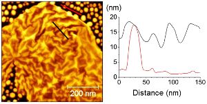 |
|
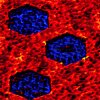
The AFM image shows a graphene/metal nanoparticle hybrid material fabricated by transferring
graphene onto closely spaced gold nanoparticles produced on a silica wafer.
Graphene is highly rippled and suspended between nanoparticles.
This study shows that the graphene Raman peaks are enhanced by a factor which depends
on the excitation wavelength, in accordance with the surface plasmon resonance
of the gold nanoparticles, and also on the graphene nanoparticle distance which is tuned
by annealing at moderate temperatures.
Scanning tunneling microscopy and spectroscopy (STM/STS) measurements show that the
local density of electronic states in graphene is modulated by the underlying gold nanoparticles.
|
Publication
>>
|
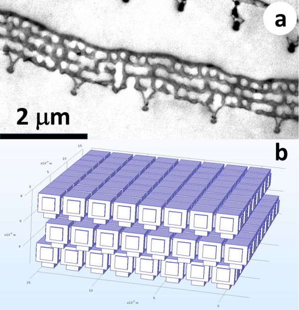
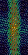
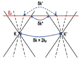
Bilayered graphene superlattices
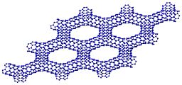 |
|
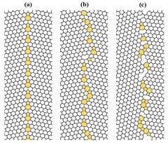
Large scale ab-initio calculations of our Russian partners within the framework of the
Faemcar EU Project
showed that if we make a hole in bilayered graphene, the edges of the two layers bend and stitch
together.
If we create many hexagonal holes in a periodic arrangement, the resulting structure
is similar to a hexagonal array of nanotubes.
Our wave packet dynamical transport calculations proved that this superstructure
can be metallic or semiconductor, depending on the size and distance of the holes.
|
Publication
>>
Publication
>>
|
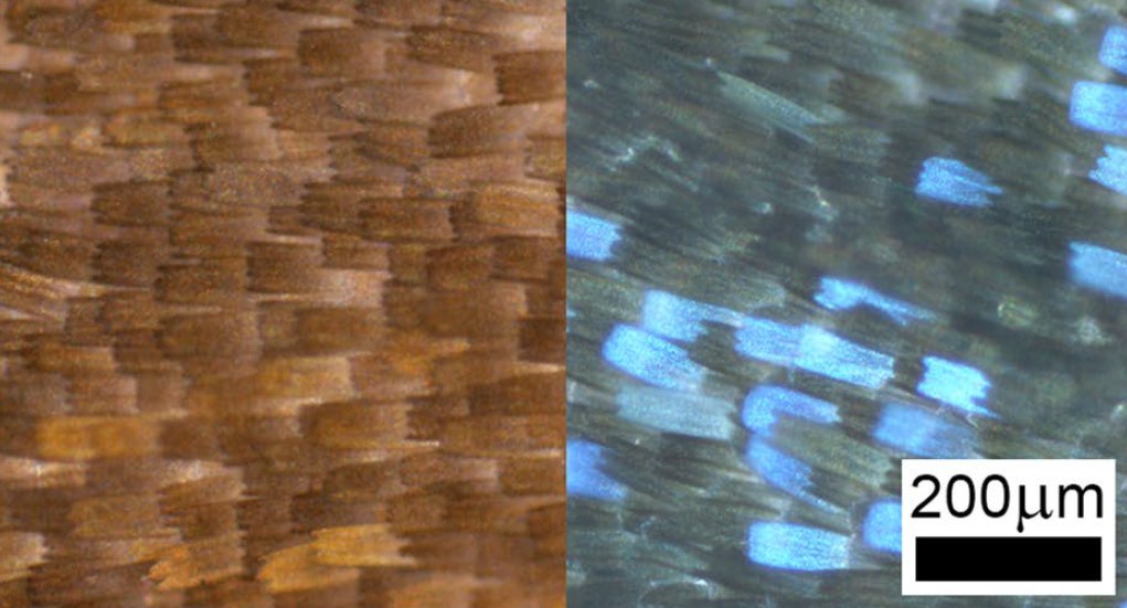
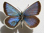
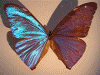
Video about an iridescent butterfly
 Left wing of this Morpho butterfly seems bright light, right wing seems brown in this image.
This otpical effect called iridescence is because the two wings were seen in different
angles when making this photo.
Iridescence, together with other interesting effects, is demonstrated
in this video.
Dr. Krisztián Kertész not only made superb photography, but he even composed and performed
the music of the video.
Left wing of this Morpho butterfly seems bright light, right wing seems brown in this image.
This otpical effect called iridescence is because the two wings were seen in different
angles when making this photo.
Iridescence, together with other interesting effects, is demonstrated
in this video.
Dr. Krisztián Kertész not only made superb photography, but he even composed and performed
the music of the video.
|
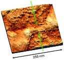
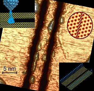
Controlling the nanoscale rippling of graphene
with SiO2 nanoparticles
 |
|
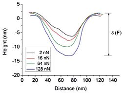
This image shows the elasticity of graphene in nano scale.
We covered an array of 25 nm diamener SiO2 nanoparticles with
a graphene sheet.
The membrane parts bridging the nanoparticles are suspended.
Then we scanned this suspended part with an AFM tip and found that
a larger force causes a larger indentation.
Revealing the details of the elastic behavior of graphene on the
nanoscale is very important for creating nanomechanical devices.
|
Publications
>> |
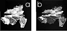
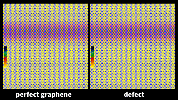
Why do
grain boundaries deteriorate the excellent properties of graphene?
 |
|
These images show the increasing disorder in
a graphene grain boundary (GB). (a) periodic; (b) "serpentine"; (c)
disordered structure. We found that the "serpentine" GB (b), though it
does not have 1D periodicity and it is not rectilinear, has similar
transport properties than the perfect periodic GB (a), while the
resistivity of the disordered GB (c) is much higher. Our calculations
show that the increased resistivity is due to the many vacancies and
4-coordinated rings, i.e. the discontinuity of the sp2
network.
|
Publications
>> |
Electric
field-controlled
rippling
of
graphene
 |
|
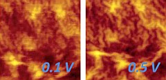
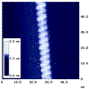
This pair of STM images was recorded on the
same 195x195 nm area of graphene, but with different voltage. Note that
the ripples, which are seen on both images are sharper on the 0.5 V
image than on the 0.1 V image. This means that the shape of the
graphene membrane can be controlled by the electric field of the STM
tip.
|
Publications
>> |
Electronic
transport
through
ordered
and
disordered
graphene
grain
boundaries
 |
|
This animation (click here
for a larger version) shows the simulated formation process of a
disordered graphene grain boundary. Such grain boundaries (GBs) are
predominant in CVD prepared graphene and considerably alter the
transport properties of the samples. We identified two main factors
governing the electronic transport through GBs:
the misorientation angle of the two adjacent graphene grains and the
atomic structure of the GB. Results show a reduced transport for the
disordered GBs, primarily attributed to electronic localized states
caused by C atoms with only two covalent bonds.
|
Publications
>> |
Grain
boundaries
in
graphene
grown
by
chemical
vapor
deposition
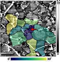
In this article written by L. P. Biró
and Ph.
Lambin the
scientific literature on graphene grain boundaries was reviewed.
Generalized conclusions were formulated, helpful for experimentalists
in interpreting the results and planning new experiments. Publications
>> |
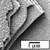
A
PhD thesis towards carbon nanotechnology
 This
image shows a graphene nanoribbon of 35 nm width and atomically
controlled edge structure. The image is from the PhD dissertation of
Peter Nemes-Incze, entitled "Nanostructures based on graphene and
functionalized carbon nanotubes". He developed several basic
methods of
producing and characterizing carbon nanostructures. This
image shows a graphene nanoribbon of 35 nm width and atomically
controlled edge structure. The image is from the PhD dissertation of
Peter Nemes-Incze, entitled "Nanostructures based on graphene and
functionalized carbon nanotubes". He developed several basic
methods of
producing and characterizing carbon nanostructures.
PhD
thesis of P.N-I, 5.4 Megabyte)
>> |
Graphene
waveguides
 If graphene is a
promising material in many respects, its remarkable
properties may be
impaired by unavoidable defects. We have undertaken electron
wave-packet dynamics calculations in a multigrain self-supported
graphene
layer. Our results show that a grain boundary may act as a reflector at
some
energies. When two grain boundaries
run parallel to each other, the graphene ribbon confined between them
may behave like a
channel for the charge carriers. We emphasize therefore the possibility
of creating nanoscale
electronic waveguides on the graphene surface by a
controlled engineering of its
grain boundaries. If graphene is a
promising material in many respects, its remarkable
properties may be
impaired by unavoidable defects. We have undertaken electron
wave-packet dynamics calculations in a multigrain self-supported
graphene
layer. Our results show that a grain boundary may act as a reflector at
some
energies. When two grain boundaries
run parallel to each other, the graphene ribbon confined between them
may behave like a
channel for the charge carriers. We emphasize therefore the possibility
of creating nanoscale
electronic waveguides on the graphene surface by a
controlled engineering of its
grain boundaries.
Publications
>>
Video
presentation
(3
min,
9
M)
>> |
The role of
structural colours as optical signals in species
recognition of butterflies
 |
This graph shows the positions of
individuals belonging to nine blue butterfly
species in the 3D color space.
This 3D graph helped us to understand, how butterflies recognize each
other, in spite of the
color of several species seems to be identical for the human eye.
These butterflies, however, posses not three, but four kind of
photoreceptors, this makes
conspecific recognation possible.
Their colors are not produced by pigments, but by nanostructures --
hence these are so called
structural colors.
Publications
>> |
|
Revealing
atomic
scale
steps
of
graphene
by
light
microscopy
 Linearly polarized light microscopy revealed
that graphene grown by chemical vapor Linearly polarized light microscopy revealed
that graphene grown by chemical vapor
deposition (CVD) on a stepped Cu substrate may appear colored.
Polarized light microscopy is an inexpensive, fast, and contamination
free method to
visualize graphene and to map the step structure of Cu substrates used
for large area CVD growth of graphene.
Publications
>> |
Mapping
the
electronic
properties
of
individual
graphene
grain
boundaries
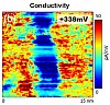
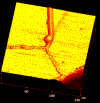
This false color tunneling conductivity map shows the electronic
structure of a graphene grain boundary. The two graphene grains (left
and right regions) are separated by a linear grain boundary (middle
region). The conductivity of the grain boundary is much lower. Graphene
grain boundaries can form p-n-p junctions with sharp interfaces of the
nm scale.
Publications
>> |
Revealing
the
grain
structure
of
graphene
This false color AFM image shows the surface of graphene grown by
chemical
vapor deposition. The colors show the orientation of the grains
determined by atomic
scale images. Publications
>> |
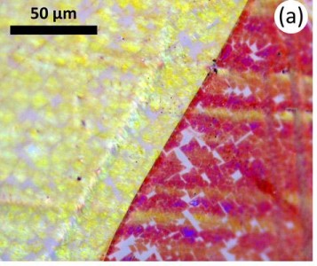
Color
based
discrimination
of
chitin-air
nanocomposites
in
butterfly
scales
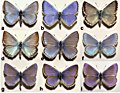 Dorsal side perpendicular view photographs of nine
investigated
Polyommatus species.
The spectral signatures of the nine species analyzed using an
artificial neural network software
show that despite the fact that all possess similar nanostructure, the
spectral
signatures exhibit enough characteristic differences to allow
the unambiguous identification of conspecific individuals.
Spectral measurements can be used as a fast
and cheap way of checking the relationships of butterfly
species in a group having common ancestry Dorsal side perpendicular view photographs of nine
investigated
Polyommatus species.
The spectral signatures of the nine species analyzed using an
artificial neural network software
show that despite the fact that all possess similar nanostructure, the
spectral
signatures exhibit enough characteristic differences to allow
the unambiguous identification of conspecific individuals.
Spectral measurements can be used as a fast
and cheap way of checking the relationships of butterfly
species in a group having common ancestry
Publications
>> |
Nanopatterning
of
graphene
with
crystallographic
orientation
control
 Computed STM image of a graphene nanoribbon with imperfect
edges.
Note the localized electronic states on the edges.
This shows the paramount importance of edge structure on the
electronic properties of graphene nanodevices.
Our recent review paper written by L. P. Biró
and Ph.
Lambin gives an up-to-date survey of methods capable of cutting
graphene with precise edge control. Computed STM image of a graphene nanoribbon with imperfect
edges.
Note the localized electronic states on the edges.
This shows the paramount importance of edge structure on the
electronic properties of graphene nanodevices.
Our recent review paper written by L. P. Biró
and Ph.
Lambin gives an up-to-date survey of methods capable of cutting
graphene with precise edge control.
Publications
>> |
Crystallographically
selective
nanopatterning
of
graphene
on
SiO
2
 Hexagonal holes of 380 nm diameter etched
into graphene layer on an
insulating surface.
Our new carbothermal etching process makes it possible to produce
graphene
nanoribbons and Y-junctions with zigzag or armchair edges. Hexagonal holes of 380 nm diameter etched
into graphene layer on an
insulating surface.
Our new carbothermal etching process makes it possible to produce
graphene
nanoribbons and Y-junctions with zigzag or armchair edges.
Publications
>>
Supplementary
Material
>> |
Colorful
beetle
as
a
model
In
nanoarchitecture
research
 During
a
lecture
Professor
Biró
gave
in
Taiwan,
he
was
shown
three
identical-looking
beetles,
but
with
different
colors.
Several
months
later,
we
revealed
a
novel
intercalated
photonic
nanoarchitecture
composed
of
a
regular
multilayer
and
nanorods
perpendicular
to
the
layers
in
the
elytra
of
this
Taiwanese
beetle
(Trigonophorus
rothschilid varians). We succeeded in producing artificial
bioinspired nanoarchitectures, with behaviors very similar to that of
the living model, by nanomachining. Our results were published in the
journal Interface
of
the
Royal
Society, and also displayed on the websites of BBC
News and Hungarian Academy of Sciences. During
a
lecture
Professor
Biró
gave
in
Taiwan,
he
was
shown
three
identical-looking
beetles,
but
with
different
colors.
Several
months
later,
we
revealed
a
novel
intercalated
photonic
nanoarchitecture
composed
of
a
regular
multilayer
and
nanorods
perpendicular
to
the
layers
in
the
elytra
of
this
Taiwanese
beetle
(Trigonophorus
rothschilid varians). We succeeded in producing artificial
bioinspired nanoarchitectures, with behaviors very similar to that of
the living model, by nanomachining. Our results were published in the
journal Interface
of
the
Royal
Society, and also displayed on the websites of BBC
News and Hungarian Academy of Sciences.
Interface
paper >>
News
on
HAS
homepage
>> |
Biological
and
bioinspired
photonic
nanoarchitectures
(a
video
talk)
 Photonic
nanostructures
exhibit
a
broad
range
of
optical
phenomena:
coloration,
iridescence,
photonic
band
gap,
polarization,
diffraction,
total
reflection,
fluorescence,
etc.
These
materials
have
many
existing
and
potential
applications
in
technology,
e.g.
in
communication,
signal
processing,
computing,
and
as
ecological
freindly
colorants.
But
biological
evolution
created
photonic
nanoarchitectures
in
living
organisms
more
than
500
Million
years
ago.
This
video
presentation
prepared
for
Hungarian Physics
Students
gives and account of our research in this field. Photonic
nanostructures
exhibit
a
broad
range
of
optical
phenomena:
coloration,
iridescence,
photonic
band
gap,
polarization,
diffraction,
total
reflection,
fluorescence,
etc.
These
materials
have
many
existing
and
potential
applications
in
technology,
e.g.
in
communication,
signal
processing,
computing,
and
as
ecological
freindly
colorants.
But
biological
evolution
created
photonic
nanoarchitectures
in
living
organisms
more
than
500
Million
years
ago.
This
video
presentation
prepared
for
Hungarian Physics
Students
gives and account of our research in this field.
Deltails
>> |
Role
of
defects
in
chemical
sensing
properties
of
carbon
nanotube
films
 As the outer
wall of the carbon nanotube plays a dominant role in the electrical
transport along the axis, the influence of the ambient on its
electrical properties offers the possibility of chemical sensing.
In our work, the modification of electrical conduction was used as the
detection principle in random networks of carbon nanotubes.
A sensor made of arc-grown SWCNTs and two others made of arc-grown
MWCNTs were also investigated.
The response of 24 different sensors to 10 vapors was studied. As the outer
wall of the carbon nanotube plays a dominant role in the electrical
transport along the axis, the influence of the ambient on its
electrical properties offers the possibility of chemical sensing.
In our work, the modification of electrical conduction was used as the
detection principle in random networks of carbon nanotubes.
A sensor made of arc-grown SWCNTs and two others made of arc-grown
MWCNTs were also investigated.
The response of 24 different sensors to 10 vapors was studied.
AVI
movie
(5
M)
>> Publications
>> |
Measuring
the
thickness
of
graphene
layers
by
TAFM
 An
Atomic Force Microscope in its "tapping mode" (TAFM) sweeps the sample
surface by an oscillating probe attached to a cantilever.
This animation shows how does the oscillation change at a step edge and
also when the material of the surface is changed below the probe tip.
We determined what TAFM imaging parameters are necessary to measure the
thickness of thin (< 1 nm) FLG (Few Layer Graphene)
layers correctly. An
Atomic Force Microscope in its "tapping mode" (TAFM) sweeps the sample
surface by an oscillating probe attached to a cantilever.
This animation shows how does the oscillation change at a step edge and
also when the material of the surface is changed below the probe tip.
We determined what TAFM imaging parameters are necessary to measure the
thickness of thin (< 1 nm) FLG (Few Layer Graphene)
layers correctly.
AVI
movie (2 M) >> Publications
>> |
Tailor-made
graphene
nanoribbons
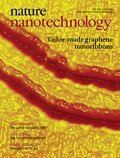 Results
of
the
Nanostructure
Department
of
the
Research
Institute for Technical
Physics and Materials Science of the Hungarian Academy of Sciences
were selected as cover page illustration for the July issue
of Nature
Nanotechnology (IF: 14.9). According to the Editor, the special
importance of the achievements of Tapasztó et al. is that they
propose solutions for two major challenges of nanoelectronic circuit
manufacturing: the engineered, precise cutting of nanometer size
circuit elements and their controlled connecting. A nano-knee ribbon is
shown on the cover page of Nature Nanotechnology, two grapheme
nanoribbons of only 8 nanometers in width connected with each other
under an angle of 30 degreed (the region between the thick red lines). Results
of
the
Nanostructure
Department
of
the
Research
Institute for Technical
Physics and Materials Science of the Hungarian Academy of Sciences
were selected as cover page illustration for the July issue
of Nature
Nanotechnology (IF: 14.9). According to the Editor, the special
importance of the achievements of Tapasztó et al. is that they
propose solutions for two major challenges of nanoelectronic circuit
manufacturing: the engineered, precise cutting of nanometer size
circuit elements and their controlled connecting. A nano-knee ribbon is
shown on the cover page of Nature Nanotechnology, two grapheme
nanoribbons of only 8 nanometers in width connected with each other
under an angle of 30 degreed (the region between the thick red lines).
Publications
>> |
Bioinspired
photonic
crystals
 Top view
Scanning Electron Microscope image of a multilayer structure
made from SiO layers and 50 nm Indium spheres (the multilayer was
broken to reveal the internal layers). This structure succesfully
reproduces the optical properties of Albulina Metallica
butterfly wing scales. Top view
Scanning Electron Microscope image of a multilayer structure
made from SiO layers and 50 nm Indium spheres (the multilayer was
broken to reveal the internal layers). This structure succesfully
reproduces the optical properties of Albulina Metallica
butterfly wing scales.
Publications
>> |
Making
of
graphene
layers
from
oxidation
of
graphite
plates
 These
3x3
um
Atomic
Force
Microscopy
images
show
the
effect
of
thermal
oxidation
on
a
few-layer
graphite
platelet
(a).
We
showed
that
such
platelets
can
be
thinned
by
thermal
oxidation
in
air,
and
individual
graphene
layers
can
be
formed
(b). These
3x3
um
Atomic
Force
Microscopy
images
show
the
effect
of
thermal
oxidation
on
a
few-layer
graphite
platelet
(a).
We
showed
that
such
platelets
can
be
thinned
by
thermal
oxidation
in
air,
and
individual
graphene
layers
can
be
formed
(b).
Publications
>> |
Switchable
biological
mirror
of
the
tortoise
beetle
 The
tortoise
beetle
Charidotella
egregia
is
able
to
modify
the
structural
color
of
its
cuticle
reversibly,
when
disturbed
by
stressful
external
events.
The
gold
coloration
displayed
by
animals
at
rest
arises
from
a
chirped
multilayer
reflector
maintained
in
a
perfect
coherent
state
by
the
presence
of
special
body
liquid
in
the
porous
patches
within
each
layer,
while
the
red
color
displayed
by
disturbed
animals
results
from
the
destruction
of
this
reflector
by
the
expulsion
of
the
liquid
from
the
porous
patches,
turning
the
multilayer
into
a
translucent slab that leaves an unobstructed view of the deeper-lying,
pigmented red substrate. The
tortoise
beetle
Charidotella
egregia
is
able
to
modify
the
structural
color
of
its
cuticle
reversibly,
when
disturbed
by
stressful
external
events.
The
gold
coloration
displayed
by
animals
at
rest
arises
from
a
chirped
multilayer
reflector
maintained
in
a
perfect
coherent
state
by
the
presence
of
special
body
liquid
in
the
porous
patches
within
each
layer,
while
the
red
color
displayed
by
disturbed
animals
results
from
the
destruction
of
this
reflector
by
the
expulsion
of
the
liquid
from
the
porous
patches,
turning
the
multilayer
into
a
translucent slab that leaves an unobstructed view of the deeper-lying,
pigmented red substrate.
Publications
>> |
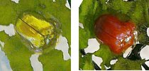
Photonic
single-
and
polycrystal
structures
on
butterfly
wings
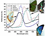
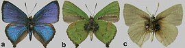 This
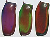
image shows the dorsal (a) and ventral (b) surface of the Cyanophrys
remus butterfly together with the ventral surface of an old,
bleached exemplar (c).
With a detailed experimental and theoretical study we showed that while
the bright metallic blue dorsal color is caused by photonic single
crystal scales, the matt green ventral color is the result of a
photonic polycrystal structure. The bleached color (c) is caused by the
decay of the absorbing pigment with time. This
image shows the dorsal (a) and ventral (b) surface of the Cyanophrys
remus butterfly together with the ventral surface of an old,
bleached exemplar (c).
With a detailed experimental and theoretical study we showed that while
the bright metallic blue dorsal color is caused by photonic single
crystal scales, the matt green ventral color is the result of a
photonic polycrystal structure. The bleached color (c) is caused by the
decay of the absorbing pigment with time.
Publications
>> New
Scientist
>> |
Carbon
nanotube
defects
imaged
by
STM
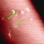 15x15
nm
atomic
resolution
STM
image
of
a
multi-wall
carbon
nanotube
(MWCNT)
showing
individual
atomic-scale
defects
caused
by
Ar
ion
irradiation.
The
defects
appear
as
hillocks
which
is
due
to
the
increased
tunneling
current
at
the
defect
sites.
Electronic
superstructures
can
be
observed
in
the
vicinity
of
the
defect
sites
with
the
period
larger
than
the
period
of
the
atomic
structure.
(Shown
by
green
lines.)
The
superstructures
appear
due
to
the
redistribution
of
the
local
density
of
states
(LDOS). 15x15
nm
atomic
resolution
STM
image
of
a
multi-wall
carbon
nanotube
(MWCNT)
showing
individual
atomic-scale
defects
caused
by
Ar
ion
irradiation.
The
defects
appear
as
hillocks
which
is
due
to
the
increased
tunneling
current
at
the
defect
sites.
Electronic
superstructures
can
be
observed
in
the
vicinity
of
the
defect
sites
with
the
period
larger
than
the
period
of
the
atomic
structure.
(Shown
by
green
lines.)
The
superstructures
appear
due
to
the
redistribution
of
the
local
density
of
states
(LDOS).
Publications
>> |
Spray pyrolysis production of CNTs
 This 10 um SEM image shows
carbon nanotubes produced by the spray
pyrolysis method.
This method is based on the simultaneous injection of a
metallocene-hydrocarbon solution through a sprayer into the reaction
furnace. Major advantage of is the direct and continuous generation of
fresh catalytic particles throughout the entire growth cycle. This
gives the possibility to scale up the method for continuous or
semicontinuous production of carbon nanotubes at commercially viable
prices. This 10 um SEM image shows
carbon nanotubes produced by the spray
pyrolysis method.
This method is based on the simultaneous injection of a
metallocene-hydrocarbon solution through a sprayer into the reaction
furnace. Major advantage of is the direct and continuous generation of
fresh catalytic particles throughout the entire growth cycle. This
gives the possibility to scale up the method for continuous or
semicontinuous production of carbon nanotubes at commercially viable
prices.
Details
>> Publications
>> |
BioPhot
Symposium
2005
 "Complexity and
evolution of photonic
nanostructures in bioorganism: templates for material sciences", 23.
Sept. 2005, Budapest "Complexity and
evolution of photonic
nanostructures in bioorganism: templates for material sciences", 23.
Sept. 2005, Budapest
Details
>> |
Hungarian
Nanotechnology
Symposium
2005
 HUNS-2005
(MANS-2005)
is
a
national
"Mobilization
Workshop"
organized
within
the
framework
of
EU
FP6
NENAMAT
project. HUNS-2005
(MANS-2005)
is
a
national
"Mobilization
Workshop"
organized
within
the
framework
of
EU
FP6
NENAMAT
project.
Details
>> |
Photonic
crystals
in
plants
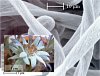 This SEM
image shows the filaments covering the leaflets surrounding
Edelweiss (see inset) bracts.
The fine structure of the filaments is a photonic crystal structure,
one of the few examples of photonic structure found in a plant.
Calculations support the idea that this wooly layer absorbs near-UV
light
before it reaches the cellular tissue. This SEM
image shows the filaments covering the leaflets surrounding
Edelweiss (see inset) bracts.
The fine structure of the filaments is a photonic crystal structure,
one of the few examples of photonic structure found in a plant.
Calculations support the idea that this wooly layer absorbs near-UV
light
before it reaches the cellular tissue.
Publications
>> |
Wing
scale
nanostructure
in
butterflies
 Our
studies
of
buttefly
wing
scale
micro-
and
nanostructure
by
electron
microscopy
show
that
structural
color
manipulation
is
a
general
instrument
in
the
evolution
of
butterflies.
Our
study
has
revealed
a
deep
interwining
between
physics
and
biology. Our
studies
of
buttefly
wing
scale
micro-
and
nanostructure
by
electron
microscopy
show
that
structural
color
manipulation
is
a
general
instrument
in
the
evolution
of
butterflies.
Our
study
has
revealed
a
deep
interwining
between
physics
and
biology.
Details
>> Publications
>> |
Biological
photonic
crystals
 This animation shows
the variation of the
iridescent color
of a butterfly as the angle of incident light is changed.
This phenomenon is caused by the photonic crystal microstructure
of the wing scales.
We measure the optical and thermal properties of the wings
and study their microstructure by SEM and TEM. This animation shows
the variation of the
iridescent color
of a butterfly as the angle of incident light is changed.
This phenomenon is caused by the photonic crystal microstructure
of the wing scales.
We measure the optical and thermal properties of the wings
and study their microstructure by SEM and TEM.
Details
>> Publications
>> |
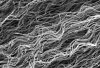
Coiled
nanotubes
 A coiled
single wall carbon nanotube is shown on this
STM image. There are certain catalyst and reaction conditions,
which enhance the formation of regularly coiled structures.
This may have to do with the formation ratio and the annealing
out of pentagon (5) and heptagon (7) rings as compared
to hexagons (6). This ratio can be influenced by the proper
combination of growth conditions, The annealing out of
5, 7 rings may be avoided by the using of the low reaction
temperatures typical for the CVD process, while the high
temperatures used in the arc growth anneal out the 5,
7 rings. A coiled
single wall carbon nanotube is shown on this
STM image. There are certain catalyst and reaction conditions,
which enhance the formation of regularly coiled structures.
This may have to do with the formation ratio and the annealing
out of pentagon (5) and heptagon (7) rings as compared
to hexagons (6). This ratio can be influenced by the proper
combination of growth conditions, The annealing out of
5, 7 rings may be avoided by the using of the low reaction
temperatures typical for the CVD process, while the high
temperatures used in the arc growth anneal out the 5,
7 rings.
Publications
>> |
Y-connections
 An Y-connection
of single wall carbon nanotubes is shown
on this STM image. Our group was the first to observe
SWNT Y-connections predicted earlier theoretically. An Y-connection
of single wall carbon nanotubes is shown
on this STM image. Our group was the first to observe
SWNT Y-connections predicted earlier theoretically.
Publications
>> |
Continuous
nanotube
production
in
underwater
arc
Multi-wall carbon nanotubes are produced by generating
an AC electric arc between two identical carbon rods,
submerged in deionized water.
Details >> Publications
>> |
|
Three body problem in three layer graphene
|
|
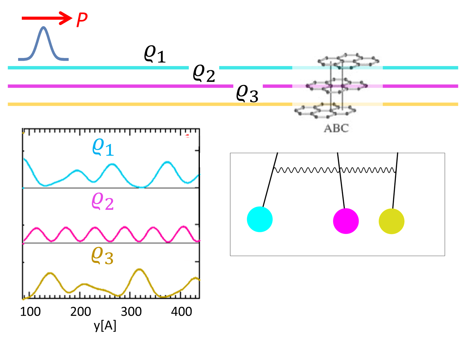
When an electronic wave packet is propagating in rhombohedral three-layer graphene, it hops between the layers (shown by different colors) in an aperiodic fashion in certain energies.
The hopping dynamics of this quantum mechanical system is similar to a simple classical system, three coupled pendulums.
Such aperiodic behavior is typical of a
3-body system
.
This massive wave packet dynamical calculation, including many thousands of atoms, was made possible by our new Carbon pseudopotential.
|
Publication
>>
Video talk about the pseudopotential
>>
Video talk about the wave packet dynamical calculation
>>
|
Hexagonal scattering of Bloch waves on a graphene defect
|
|
Left pane of this animation shows that an electronic wave packet constructed from Bloch waves travels
unhindered on a graphene surface.
The right pane shows that a structural defect causes scattering to the wave packet.
Note that the scatteing pattern is not circular, but hexagonal.
Such calculations help us understand the Scanning Tunneling Microscopy images of 2D materials
containing structural defects.
|
Publication
>>
|
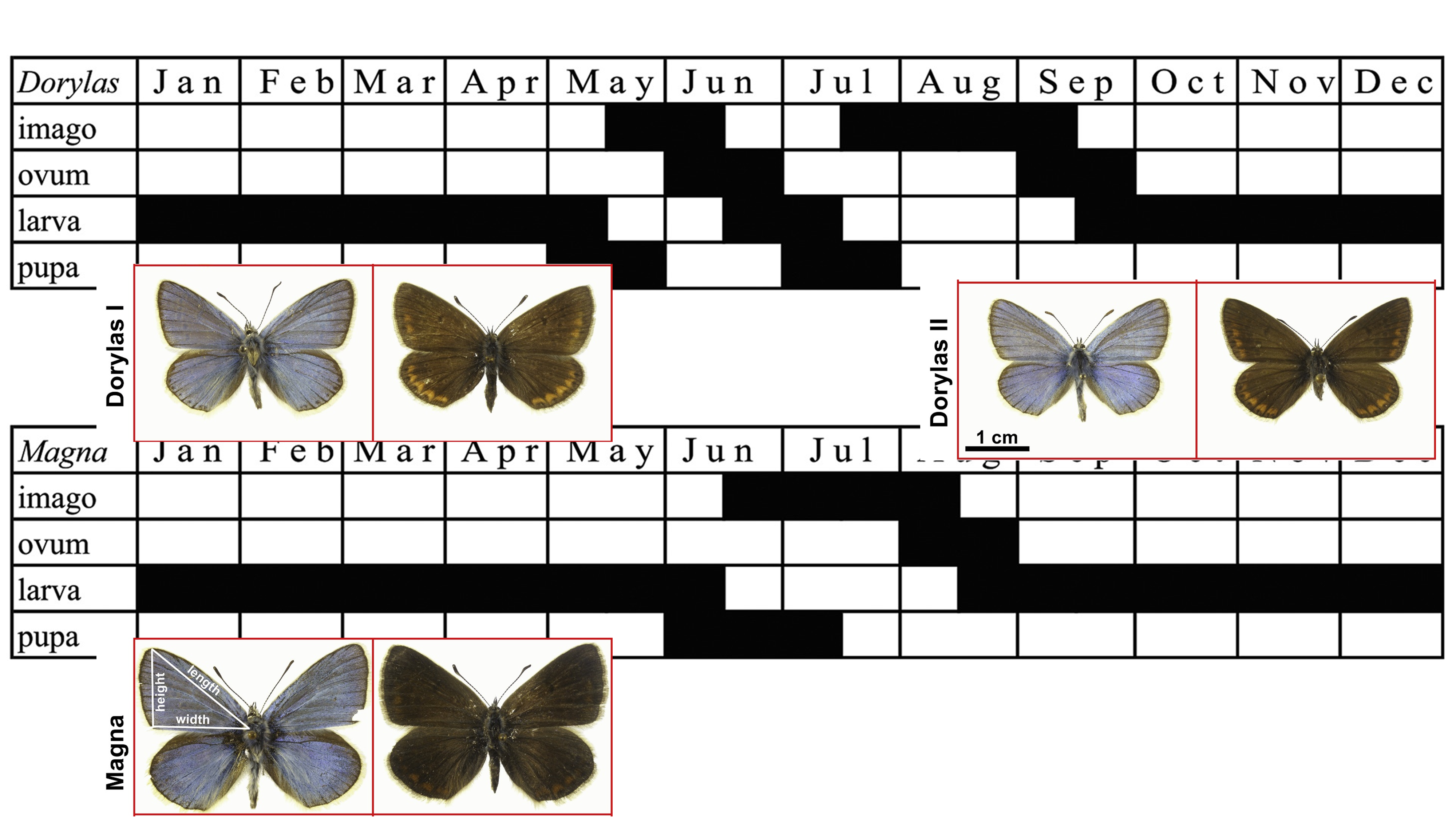
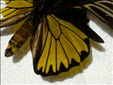
Structural color is the same in lowland and mountainous populations of Polyommatus dorylas,
despite their size differences
 |
|
This figure shows the generations and photos (male and female) of two different populations
of the same butterfly species, Polyommatus dorylas (Turquoise blue).
The lowland population (Dorylas, upper row) has two generations each year, but the mountainous population
(Magna, lower row)
has only one generation (note the winter hybernation of the larvae).
As you can see on the photos, Magna exemplars are larger, than Dorylas I and Dorylas II examplars.
Our detailed studies showed that the size of the wing scales correlate with the body size,
but the dimensions of the photonic nanostructures generating the conspicious blue color remain constant.
Hence the optical spectrum is the same for the two populations.
This proves that the dimensions of the photonic nanostructure are genetically determined,
because the structural color is an important species-specific trait.
|
Publication
>>
|
Web-Schrödinger
3.2
 |
|
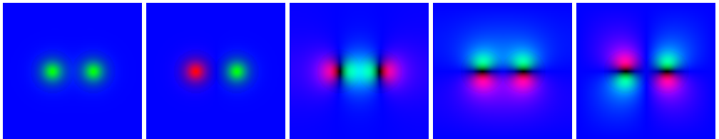
Web-Schrödinger is a program for the interactive
solution of the time dependent and stationary two dimensional (2D)
Schrödinger
equation. The program itself runs on our server and can be used through
the Internet with a simple Web browser.
The new 3.2 version makes it possible to use piecewise linear and quadratic potentials,
as demonstrated on this simple model of a diatomic molecule.
|
Details
>>
|
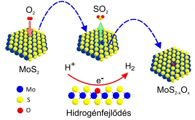
Increased catalytic activity in 2D MoS2-xOx crystals
 |
|
The chemical inertness of the defect-free basal plane confers environmental stability to
MoS2 single layers, but it also limits
their chemical versatility and catalytic activity.
The stability of pristine MoS2 basal plane against oxidation under ambient conditions
is a widely accepted assumption however,
L. Tapaszto et. al. recently reported in
Nature Chemistry
single-atom-level structural investigations that reveal that
oxygen atoms spontaneously incorporate into the basal plane of MoS2 single layers
during ambient exposure.
The use of scanning tunnelling microscopy reveals a slow oxygen-substitution reaction,
during which individual sulfur atoms are replaced one
by one by oxygen, giving rise to solid-solution-type 2D MoS2-xOx crystals.
Oxygen substitution sites present all over the basal
plane act as single-atom reaction centres, substantially increasing the catalytic activity
of the entire MoS2 basal plane for the
electrochemical H2 evolution reaction.
|
|
Electronic dynamics in graphene and MoS2 systems
 |
|
This computer simulated image shows a snapshot from the time development of an electronic wave packet
injected into the surface of a molybdenum disulfide (MoS2) sheet from the apex of a Scanning Tunneling Microscope tip.
Studying the evolution of a packet of electrons having their momentum distributed around a given
value gives information on the transport properties of the material.
This approach has been used for graphene and MoS2.
Due to its complex band structure MoS2 presents an interesting dynamics for electrons.
|
Publication
>>
|
Biological variability of butterfly colors
 |
|
These two butterfly specimens, Polyommatus icarus (A, Common Blue) and Plebejus argus (B, Silver-studded Blue) collected in Hungary (scale bar 10 mm)
have similar color to the human eye, but their near UV spectra are different.
Despite living in the same type of habitat, these two species display differences in prezygotic mating strategy:
the males of P. icarus are patrolling, while P. argus males have sedentary behavior.
Therefore, the species-specific photonic nanoarchitecture, which is the source of the structural
coloration, may have been subjected to different evolutionary effects.
The structural
coloration of the four wings of 25 male individuals (100 samples for each species) was measured.
Significant differences were found in the near UV wavelength region that are
perceptible by these polyommatine butterflies but are invisible to human observers.
|
Publication
>>
|
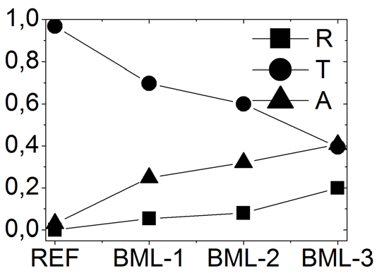
Hot pressed nanocarbon-plastic composites for electromagnetic shielding
 |
|
This graph shows the Reflection, Transmission, and Absorption of a 30 um thick
nanocarbon-PLA (poly lactic acid) composite as the function of nanocarbon content
for 30 GHz microwave radiation.
The electromagnetic shielding efficiency increases with increasing amount of
nanocarbon in the layer.
3D printing combined with hot pressing is a low cost method to create
light-weight and enviromentally friendly electromagnetic shielding layers active
in a broad frequency range.
|
Publication
>>
|
Wave packet dynamics -- different methods for different scenarios
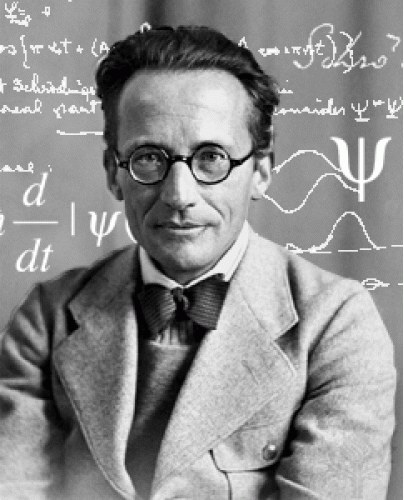
Erwin Schr dinger introduced the concept of wave packets in 1926 to bridge the gap between
classical and quantum mechanics.
The wave packet dynamical method is a scattering experiment inside the computer: an incoming
wave packet is "shot" into the physical system and the time development of the packet is calculated.
We presented a detailed analysis of different techniques of wave packet dynamical calculations
for carbon nanostructures in this book chapter, including Schr dinger equation, Dirac equation,
jellium potential, pseudopotential, and multidomain methods.
Publication
>>
|
3D printed nanocarbon sandwich structures
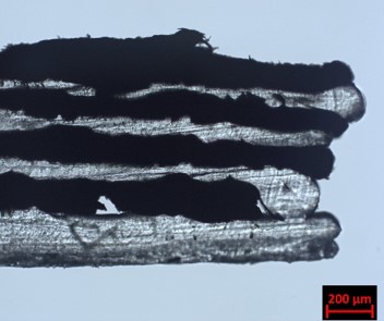 |
|
We constructed a new type of light-weight material by 3D printing of nano-carbon doped
plastic layers and pure plastic layers -- see the cross sectional optical microscopy image
above.
Sandwich structures containing only two nanocarbon layers already become not transparent
to the microwaves.
By such combination of conductive and dielectric materials we can easily realize photonic crystal
like structures active in the microwave (GHz) and THz range.
These studies serve as a basis for design and realization of optimal geometries of meta-surface type,
in order to reach a high level of electromagnetic interference shielding performance
for EM cloaking and EM ecology applications.
|
Publication
>>
|
|
Room temperature magnetic order on zigzag edges of narrow graphene nanoribbons
 Experimental data reveal the emergence of magnetic order on edges of sub-10 nm graphene nanoribbons. Using a nanofabrication technique based on Scanning Tunneling Microscopy Lithography, graphene nanoribbons have been fabricated with nanometer precision and edges of well-defined crystallographic orientation. Ribbons with edges of so-called zigzag orientation display a sharp semiconductor-metal transition as a function of their width, which was identified as the signature of a magnetic switching from antiferromagnetic to ferromagnetic coupling between spin-polarized ribbon edges. Remarkably the edge magnetism was found to be stable at room temperature, raising hopes of graphene-based spintronic devices operating under ambient conditions. The results have been published in the October 30th issue of
Nature.
Experimental data reveal the emergence of magnetic order on edges of sub-10 nm graphene nanoribbons. Using a nanofabrication technique based on Scanning Tunneling Microscopy Lithography, graphene nanoribbons have been fabricated with nanometer precision and edges of well-defined crystallographic orientation. Ribbons with edges of so-called zigzag orientation display a sharp semiconductor-metal transition as a function of their width, which was identified as the signature of a magnetic switching from antiferromagnetic to ferromagnetic coupling between spin-polarized ribbon edges. Remarkably the edge magnetism was found to be stable at room temperature, raising hopes of graphene-based spintronic devices operating under ambient conditions. The results have been published in the October 30th issue of
Nature.
The Nature paper
>>
|
Substance specific chemical sensing with butterfly wing scales
 |
|
This image shows the color change of the butterfly scale in our vapor sensing experiments
in the 3D chromaticity diagram using 7 vapors at 10 concentrations.
We proved that a modification of the surface may offer a possibility to
sensitize / desensitize the sensors for certain volatiles and to produce sensor
arrays.
Interestingly we found that the evaluation of color changes induced by the different vapors
in the 3D visual space of the butterflies
(
The role of structural colours as optical signals in species recognition of butterflies)
and by Principal Component Analyis (PCA) results in alsmost perfectly coincident trajectories.
It is remarkable that a color generating biologic nanoarchitecture, evolved in the scales,
and its receptor: the butterfly eye, and a purely matehmatical algorithm yielded the
very same result.
|
Publications
>> |
"Highlights of 2013" Award
 This
award
certifies that the article
Grain boundaries in graphene grown by chemical vapor deposition
by
L. P. Biró
and Ph.
Lambin
has been selected by the editors of
New Journal of Physics
for inclusion
in the exclusive Highlights of 2013 collection. Papers are chosen on the basis of
referee endorsement, novelty, scientific impact and broadness of appeal.
This
award
certifies that the article
Grain boundaries in graphene grown by chemical vapor deposition
by
L. P. Biró
and Ph.
Lambin
has been selected by the editors of
New Journal of Physics
for inclusion
in the exclusive Highlights of 2013 collection. Papers are chosen on the basis of
referee endorsement, novelty, scientific impact and broadness of appeal.
|
MFA Yearbook 2013
 Pages 22-24 and 46-58
of the
2013 Yearbook
of the
Institute of Technical Physics and Materials Science
gives a good overview of the work of our Nanostructures Laboratory,
but the whole Yearbook is worth to read,
as well as the
previous ones!
Pages 22-24 and 46-58
of the
2013 Yearbook
of the
Institute of Technical Physics and Materials Science
gives a good overview of the work of our Nanostructures Laboratory,
but the whole Yearbook is worth to read,
as well as the
previous ones!
2013 Yearbook, PDF, 52M
>>
|
Gas sensing with butterfly wings
 This animation shows the reversible color change of a butterfly wing
when ethanol is
dripped on it.
Our results showed that a color change also occurs when the wing is
exposed
to different vapors.
This small color change is well measurable in the optical spectrum, the
spectrum
transition is fast and linear for small concentrations.
These features make biological photonic crystals a potential candidate
for a cheap gas sensor material.
This animation shows the reversible color change of a butterfly wing
when ethanol is
dripped on it.
Our results showed that a color change also occurs when the wing is
exposed
to different vapors.
This small color change is well measurable in the optical spectrum, the
spectrum
transition is fast and linear for small concentrations.
These features make biological photonic crystals a potential candidate
for a cheap gas sensor material.
Publications
>> |
Bioinspired
disordered
photonic
nanoarchitectures
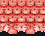
 This image shows a model of a so called 1+2D nanostructure:
we deposited a multilayer structure on an array of nanospheres. This
bioinspired nanoarchitecture shows peculiar optical properties:
both specular and diffuse reflection. This image shows a model of a so called 1+2D nanostructure:
we deposited a multilayer structure on an array of nanospheres. This
bioinspired nanoarchitecture shows peculiar optical properties:
both specular and diffuse reflection.
Publications
>> |
Color
changes upon cooling of butterflies
 |
|
These images show the different response of
butterfly wings upon cooling, depending on whether the color is given
by a photonic nanostructure containing open nanovoids or a pigment. The
effect is caused by water vapor condensation.
|
Publications
>> |
Electronic
states
of
disordered
grain
boundaries
in
graphene
 |
|
This pair of Scanning Tunneling Microscope
(STM) images shows an ordered and a disordered grain boundary (GB) in
graphene. (Ordered: J.Cervenka et al, disordered: our measurement).
Such disordered GBs are often seen in graphene samples prepared by CVD,
hence we studied their properties by experimental and theoretical
methods. This is important for nanoelectronic applications of graphene.
|
Publications
>> |
Selective
etching
of
armchair
edges
in
graphite
 |
|
Due to its high electron mobility and long
coherence length, graphene is a promising material for next generation
electronic devices. Patterning graphene with well controlled
crystallographic orientation and atomically precise edges is very
important for such applications. Formerly,
we
developed
a
method
for
producing
graphene
edges
with
zigzag
orientation,
and
our
new
procedure
makes
it
now
possible
to
etch
edges
with
armchair
orientation.
|
Publications
>> |
Web-Schrödinger
3.0
 Web-Schrödinger is a program for the interactive
solution of the time dependent and stationary two dimensional (2D)
Schrödinger
equation. The program itself runs on our server and can be used through
the Internet with a simple Web browser. The stationary states
calculation is new in this version 3.0. Web-Schrödinger is a program for the interactive
solution of the time dependent and stationary two dimensional (2D)
Schrödinger
equation. The program itself runs on our server and can be used through
the Internet with a simple Web browser. The stationary states
calculation is new in this version 3.0.
Details
>> Publications
>> |
Nanoscale
ripples
on
graphene
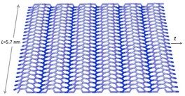 |
|
L. Tapaszto and coworkers realized
subnanometre-wavelength periodic
ripples of suspended graphene membranes.
The observed nanorippling mode violates
the predictions of the continuum model.
Nevertheless, microscopic simulations based on
a quantum mechanical description of the chemical binding
accurately describe the observed rippling mode.
The ability of graphene to ripple down to subnanometre
wavelengths can be exploited in strain-engineering graphene-based
nanoelectronic and nanoelectromechanical devices beyond the
boundaries set by continuum mechanics.
|
Publications
>> |
Graphene:
nanoscale
processing
and
recent
applications
 |
|
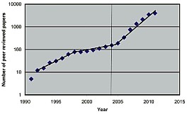
This image shows the number of graphene
related publications for the years 1990-2011 in logarithmic scale. The
fast evolution of research made possible the preparation of samples
with arbitrary sizes. Available sample production techniques, combined
with the right patterning tools, can be used to tailor the graphene
sheet into functional nanostructures, even whole electronic circuits.
Our review paper gives a survey of existing graphene patterning
techniques and potential applications of related lithographic methods.
|
Publications
>> |
Dynamical
analysis
of
the
STM
tip
--
graphene
tunneling
event
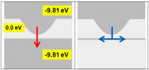 This pair of images shows two situations: when
the electron is tunneling from the tip of a Scanning Tunneling
Microscope into a bulk sample (left)
and when it is tunneling into a thin layer (right), like graphene. In the
case of the bulk sample the direction of the momentum of the electron (red arrow) does not change, but
for the thin layer the momentum (blue
arrow) has to change direction. We analyzed this phenomenon, together
with other important effects influencing the STM imaging mechanism of
graphene. This pair of images shows two situations: when
the electron is tunneling from the tip of a Scanning Tunneling
Microscope into a bulk sample (left)
and when it is tunneling into a thin layer (right), like graphene. In the
case of the bulk sample the direction of the momentum of the electron (red arrow) does not change, but
for the thin layer the momentum (blue
arrow) has to change direction. We analyzed this phenomenon, together
with other important effects influencing the STM imaging mechanism of
graphene.
Publications
>> |
Anisotropic
dynamics
of
charge
carriers
in
graphene
 |
|
This animation (click
to
enlarge) shows the
time evolution of an electron wave packet on the graphene surface. The
wave packet is inserted from a simulated Scanning Tunneling Microscope
tip (see the left image, a vertical cross section). The right image
(horizontal cross section) shows a peculiar anisotropic dynamics, which
may have important applications in future graphene nanodevices.
|
Publications
>> |
Parallel
nanolitography
 This
STM image shows two graphene nanoribbons etched by a double tip
with two apexes situated about
31 nm apart from each other.
Parallel processing is of utmost importance if practically relevant
nanocircuitry from graphene is targeted.
We examined parallel processing of graphene by scanning tunneling
lithography (STL) and
by carbothermal etching (CTE). This
STM image shows two graphene nanoribbons etched by a double tip
with two apexes situated about
31 nm apart from each other.
Parallel processing is of utmost importance if practically relevant
nanocircuitry from graphene is targeted.
We examined parallel processing of graphene by scanning tunneling
lithography (STL) and
by carbothermal etching (CTE).
Publications
>> |
Energy
resolved tunneling conductance mapping of
functionalized carbon nanotubes
 The
upper image is a schematic illustration of our novel CNT immobilization
technique, which facilitates the study the topography and electronic
structure of functionalized
CNTs by STM.
The technique is based on incorporating the functionalized multiwalled
CNTs into
a few-layer graphene-nanotube composite, as shown on the lower STM
image.
Our measurements illustrate the advantage energy resolved tunneling
conductance maps can give,
namely to spot sample features that are not apparent from STM
topography maps and to provide
information on local functionalization and doping. The
upper image is a schematic illustration of our novel CNT immobilization
technique, which facilitates the study the topography and electronic
structure of functionalized
CNTs by STM.
The technique is based on incorporating the functionalized multiwalled
CNTs into
a few-layer graphene-nanotube composite, as shown on the lower STM
image.
Our measurements illustrate the advantage energy resolved tunneling
conductance maps can give,
namely to spot sample features that are not apparent from STM
topography maps and to provide
information on local functionalization and doping.
Publications
>> |
Photonic
nanoarchitectures
in
butterflies
and
beetles
--
a
review
Nature
began developing photonic nanoarchitectures millions of years before
humankind. In their review paper, L. P. Biró
and J.-P.
Vigneron, present a survey of the development of natural photonic
crystal-type nanoarchitectures occurring in butterflies and beetles
from the standpoint of physics and materials science The
characterization, modeling methods, and rapidly growing number of
bioinspired or biomimetic applications are discussed.
Publications
>> |
Raman
scattering on graphene zigzag edges
| |
|
Theory has predicted rich and very distinct
physics for graphene nanodevices with boundaries that follow either the
armchair or the zigzag crystallographic directions. We have
demonstrated that hexagonal holes obtained by anisotropic etching of
graphene are bounded predominantly by zigzag edges which do not
contribute to the D peak in Raman spectroscopy.
|
Publications
>> |
Graphene
by
HOPG
fluorination
and
water
vapor
reduction
 STM image (size 3 nm) of the surface of fluorinated
graphite in ambient
air.
Graphite fluoride was obtained by fluorination of highly oriented
pyrolytic graphite (HOPG) by a gaseous mixture of BrF3 and Br2.
XRD,
STM,
AFM,
Raman
spectroscopy
and
XPS
were
used
to
investigate
the
fluorination
process
and
the
reduction
of
CF2 to graphene
on interaction with water vapor.
It was found that the crystallinity of the topmost graphene layer
produced by reduction is superior as compared to oxidation exfoliated
graphene. STM image (size 3 nm) of the surface of fluorinated
graphite in ambient
air.
Graphite fluoride was obtained by fluorination of highly oriented
pyrolytic graphite (HOPG) by a gaseous mixture of BrF3 and Br2.
XRD,
STM,
AFM,
Raman
spectroscopy
and
XPS
were
used
to
investigate
the
fluorination
process
and
the
reduction
of
CF2 to graphene
on interaction with water vapor.
It was found that the crystallinity of the topmost graphene layer
produced by reduction is superior as compared to oxidation exfoliated
graphene.
Publications
>> |
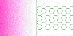
Effect
of disorder on the color of photonic crystals
 |
| This animation shows how the Fourier power
spectrum of a perfect
crystal is changing, when the lattice planes are randomly shifted.
Understanding the effect of randomness on the Fourier image helped us
to explain, how the Albulina metallica butterfly creates its
viewing angle dependent coloration by a disordered nanostructure. |
Publications
>> |
Tuning
the electronic structure of graphene by ion irradiation
 We irradiated single atomic layer graphene
sheets with Ar+ ions in
order to study the effect of defects and disorder on the electronic
structure.
The samples were investigated by STM and STS.
The most important consequence of the induced disorder is the reduction
in the Fermi velocity, as illustrated in this figure.
Hence we can tune the Fermi velocity of graphene by ion irradiation,
which could open up new perspectives for graphene electronics. We irradiated single atomic layer graphene
sheets with Ar+ ions in
order to study the effect of defects and disorder on the electronic
structure.
The samples were investigated by STM and STS.
The most important consequence of the induced disorder is the reduction
in the Fermi velocity, as illustrated in this figure.
Hence we can tune the Fermi velocity of graphene by ion irradiation,
which could open up new perspectives for graphene electronics.
Publications
>> |
Nano
Christmas
 Wish
You Merry Chrsitmas with this nano Christmas tree calculated by
Web-Schrödinger. It shows the scattering of a wave packet on a
potential forming an X-mas tree. The height of the tree is 3 nm. See
the "File / Load Example" menu of the program! Wish
You Merry Chrsitmas with this nano Christmas tree calculated by
Web-Schrödinger. It shows the scattering of a wave packet on a
potential forming an X-mas tree. The height of the tree is 3 nm. See
the "File / Load Example" menu of the program!
Details
>> Publications
>> |
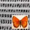
Photonic
nanoarchitectures
in
butterfly
scales
as
gas
sensors
 From 20 examined butterfly species all showed
selective gas/vapor
sensing when
various volatile organic compounds were introduced as additives in
ambient air.
Each butterfly species gives characteristic response both for species,
i.e., for its typical nanoarchitecture, and for the seven test vapors
used. Fast response time, reproducible and concentration dependent
signals are demonstrated. From 20 examined butterfly species all showed
selective gas/vapor
sensing when
various volatile organic compounds were introduced as additives in
ambient air.
Each butterfly species gives characteristic response both for species,
i.e., for its typical nanoarchitecture, and for the seven test vapors
used. Fast response time, reproducible and concentration dependent
signals are demonstrated.
Publications
>> |
Diffraction
and
fluorescence
in
the
iridescence
of
Troides
magellanus
 This birdwing butterfly lives in a restricted area of the
Philippines.
The yellow-green color of its hindwings is caused by a pigment, but as
shown on the animation,
when viewed at a specific angle, the hindwing shows a bright blue
flash.
The bright blue color is concentrated at a narrow angular range, this
ensures that it is seen only
by potential mates, but unseen by the predators.
Detailed analysis showed that this effect is caused by a blazed optical
grating on the surface of the wing scales. This birdwing butterfly lives in a restricted area of the
Philippines.
The yellow-green color of its hindwings is caused by a pigment, but as
shown on the animation,
when viewed at a specific angle, the hindwing shows a bright blue
flash.
The bright blue color is concentrated at a narrow angular range, this
ensures that it is seen only
by potential mates, but unseen by the predators.
Detailed analysis showed that this effect is caused by a blazed optical
grating on the surface of the wing scales.
Publications
>> |
Interference
of
electronic
waves
on
the
graphite
surface
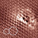 58
x
58
nm
atomic
resolution
STM
image
of
the
graphite
surface
near
the
vicinity
of
a
defect
site
created
by
ion
irradiation.
Position
dependent
superstructure
patterns
are
present
near
the
defect,
as
marked
by
the
two
circles.
Our
results
indicate
that
superstructure
patterns
are
mainly
determined
by
the
available
scattered
states
of
the
system
rather
than
the
detailed
structure
of
the
defect
site.
We
propose
an
interference
model,
which
can
explain
the
presence
of
coexisting
superstructures
both
on
graphite
and
carbon
nanotubes. 58
x
58
nm
atomic
resolution
STM
image
of
the
graphite
surface
near
the
vicinity
of
a
defect
site
created
by
ion
irradiation.
Position
dependent
superstructure
patterns
are
present
near
the
defect,
as
marked
by
the
two
circles.
Our
results
indicate
that
superstructure
patterns
are
mainly
determined
by
the
available
scattered
states
of
the
system
rather
than
the
detailed
structure
of
the
defect
site.
We
propose
an
interference
model,
which
can
explain
the
presence
of
coexisting
superstructures
both
on
graphite
and
carbon
nanotubes.
Publications
>> |
Transport
through
a
graphene
nanoribbon
 |
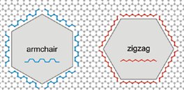
| This animation of 6 fs duration
shows the transport of an
electronic wave packet through a graphene nanoribbon. Pronounced edge
states are seen and the interference of the eigenstates of the
nanoribbon causes different patterns to appear along the CC bonds. |
Publications
>> |
BioPhot
software & database
 BioPhot
Analyzer is a program for organized storage and retrieval of images
(photographic and microscopic) and measurements of butterfly wing
scales. Butterfly specific image- and data analysis tools help the user
to understand the raw data. The software was developed by a SME, Softadmin. BioPhot
Analyzer is a program for organized storage and retrieval of images
(photographic and microscopic) and measurements of butterfly wing
scales. Butterfly specific image- and data analysis tools help the user
to understand the raw data. The software was developed by a SME, Softadmin.
Details
>> |
Imaging
electron
interference
patterns
on
MWNTs
 This
animation
shows
the
changing
of
the
calculated
STM
image
of
a
multi-wall
carbon
nanotube
(MWNT)
as
a
function
of
the
Utip
voltage applied to the STM tip.
Our new interference model accounts for the complex electron density
oscillations
near defect sites. This
animation
shows
the
changing
of
the
calculated
STM
image
of
a
multi-wall
carbon
nanotube
(MWNT)
as
a
function
of
the
Utip
voltage applied to the STM tip.
Our new interference model accounts for the complex electron density
oscillations
near defect sites.
Publications
>> |
BioPhot
Symposium
2007
"Complexity and
evolution of photonic
nanostructures in bioorganism: templates for material sciences", 24-25.
Sept. 2007, Budapest
Details
>> |
Energetics
of
CNT
bundles
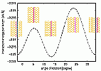 This
graph
shows
the
interaction
potential
curve
of
two
aligned
(10,10)
carbon
nanotubes
with
one
tube
fixed
and
the
other
rotating
about
its
axis.
We
studied
in
detail
the
energetics
of
CNT
pairs
and
bundles
of
CNTs. This
graph
shows
the
interaction
potential
curve
of
two
aligned
(10,10)
carbon
nanotubes
with
one
tube
fixed
and
the
other
rotating
about
its
axis.
We
studied
in
detail
the
energetics
of
CNT
pairs
and
bundles
of
CNTs.
Publications
>> |
Manhattan plot
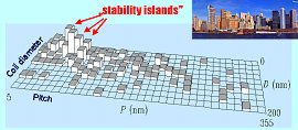 |
| The statistical distribution of a large
number of helically coiled
carbon nanotubes was analyzed in a cross-correlated way in their
geometrical configuration space defined by diameter and pitch.
Stability islands were identified, in which the number of coils exceeds
about 15-10 times the value corresponding to a uniform distribution. |
Details
>> Publications
>> |
Structural
models
for
coiled
nanotubes
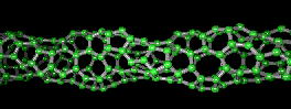 |
| By assembling azulene units (fused
pentagon-heptagon pairs) and
hexagons,
and applying specific wrapping rules to these structures resembling
some recently-proposed Haeckelite structures
(Terrones et al., Phys. Rev. Lett. 84, 1716 (2000)),
a large variety of toroidal, coiled, screwlike, and double-helix
structurescan be generated.
In these structures the ratio of nonhexagonal ringsto hexagonal units
varies from 4:1 to 4:3 by contrast to earlier coilmodels
where this ratio was well below unity. |
Publications
>> |
3D
calculation of tunneling through a SWNT in STM
 This is a snapshot from the
quantum mechanical time dependent
simulation of the tunneling of an electron wave packet
through a model of a nanotube in an STM setup. This is a snapshot from the
quantum mechanical time dependent
simulation of the tunneling of an electron wave packet
through a model of a nanotube in an STM setup.
Details
>> Publications
>> |
2D tunneling
calculations through SWNTs in STM
 This animation shows the
time development of an
electron wave packet while tunneling
through a model of a nanotube in an STM setup. This animation shows the
time development of an
electron wave packet while tunneling
through a model of a nanotube in an STM setup.
Details >>
Publications
>> |
|
|
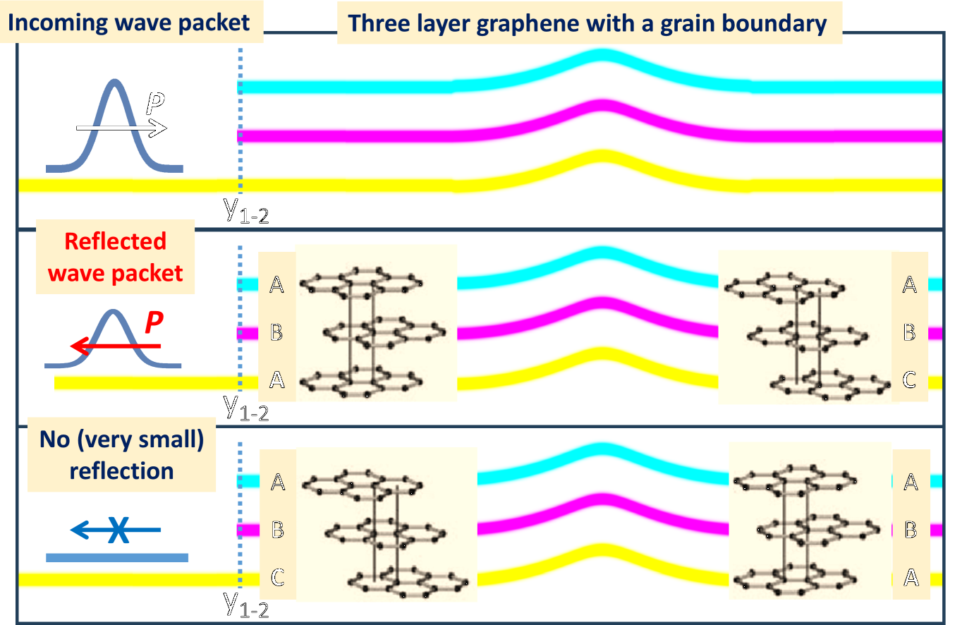
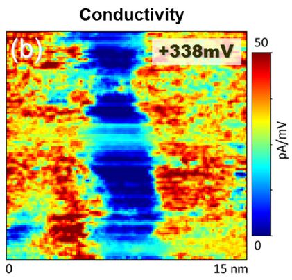
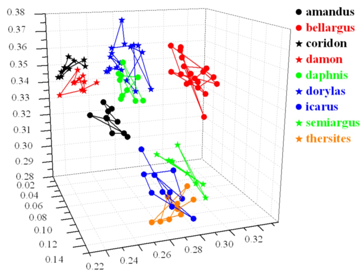