Calculation of Effects of Tunnel Junction Geometry in
Scanning Tunneling Microscopy
G. I.
MárkaInstitut fur Physik , Universitat Basel, Klingelbergstrasse 82, CH-4056 Basel, Switzerland
E. Balázs
Institute of Physics, Technical University, H-1521 Budapest, Hungary
Corresponding author: G. I. Márk , mark@sunserv.kfki.hu , Nanostructures Laboratory , MFA Research Institute for Technical Physics and Materials Science
H-1525 Budapest, P.O.Box.49., Hungary
Our other publications on STM simulation are available here.
ABSTRACT
A theoretical study of current density for the case of tunneling through phenomenological1 and variationally2 calculated metal-vacuum-metal (MVM) potential barriers is presented. The two-dimensional time dependent Schrödinger equation is solved numerically. Spectroscopic effects (e.g. the effects of low work function tip patches) as well as electron focusing effects are investigated within the framework of this model. Predictions of semiclassical calculations (e.g. geometrical asymmetries in I(V) curves) are verified.This work was partially supported by the Swiss National Science Foundation.
1 N. Garcia, C. Ocal and F. Flores, Phys. Rev. Lett. 50, 2002 (1983).
2 E. Balazs & L.Orosz, Surf. Science 238, 341 (1990).
a Permanent address: Institute of Physics, Technical University, H-1521 Budapest, Hungary
METHOD
The time dependent Schödinger equation is solved by Fourier transform method. Given an initial state Psi 0 (r) the method allows us to calculate the time evolution of the wave function. The potential seen by an electron when tunneling from one electrode to the other is approximated asV(s) = Velst(s) + Vxc(s) + Vim(s) + Voc(s)
where s is the arch length of a semiclassical WKB trajectory measured from the cathode to the actual position of the electron, Velst(s) is the electrostatic potential due to the electron density and for the exchange correlation potential the usual Wigner-formula is used. The image potential is calculated as an infinite sum. The potential Voc(s) arises from the external bias and the contact potential. The potential barrier approximated in this way aligns with that obtained in a quasi-SCF way1. In tip negative case the semiclassical trajectories were approximated by the lines of force of the electrostatic field, for tip positive biases straight lines perpendicular to the sample plane were chosen.
ASSUMPTIONS
The tip and the surface are of the same material, (Au, EF = 5.5 eV, Phi = 5.2 eV). The incident wave function is assumed to be a Gaussian wave packetRESULTS
- Tip negative current is smaller than tip positive one.
- Large spatial oscillations occur in the current in the interface region
- Influence of the tip shape seems to be important
ACKNOWLEDGEMENT
The authors express their gratitude to the IBM, Hungary for supporting their participation at this Conference.GIM gratefully acknowledges the hospitality at the Institute fur Physik, Universitat Basel, Switzerland
REFERENCES
- N. Garcia, C. Ocal and F. Flores, Phys.Rev.Letters 50(1983)2002.
- E. Balázs and L. Orosz, Surf. Sci. 238(1990)341.
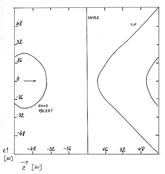 |
| FIG.1. STM model geometry.
Surface of the plane sample and the hyperbolic tip is shown together
with an iso-density line of the incoming wave packet. |
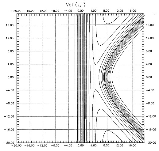 |
| FIG.2. Contours of
constant Veff(z,r).
Contour spacing is 0.02 Hartree.
Thick line: Veff = EF. |
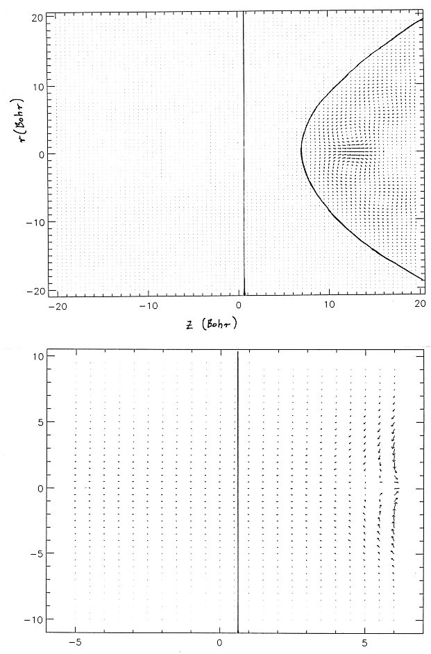 |
| FIG.3. Current density for
tip negative bias (wave packet coming from the tip). Upper figure is
for the whole model, lower figure is
for the tunneling channel. |
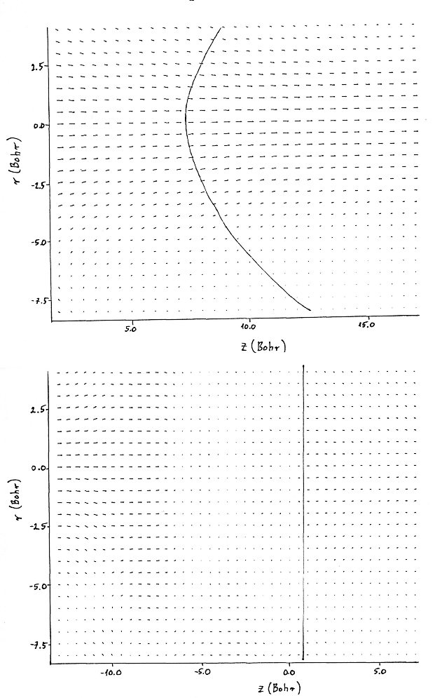 |
| FIG.4. Current density for tip positive bias (wave packet coming from the sample). Upper figure is for the whole model, lower figure is for the tunneling channel. |
 |
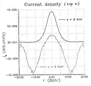 |
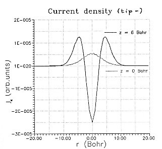
| FIG.5.a. Radial current density for tip negative bias (wave packet coming from the sample). Thick line: measured at tip apex, thin line: measured at sample surface. Oscillations are numerical artefacts. | FIG.5.a. Radial current
density for tip positive bias (wave packet
coming from the tip). Thick line: measured at tip apex, thin line:
measured at sample surface. Oscillations are numerical artefacts. |
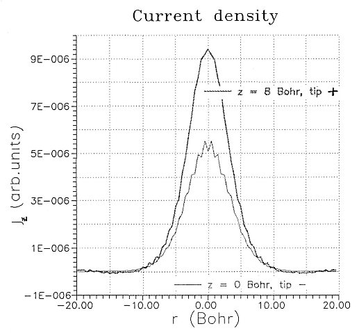 |
| FIG 6. Radial tunnel
current density measured at tip apex for tip positive case (wave packet
coming from the tip) and at sample surface for tip negative case (wave packet
coming from the sample). Oscillations at the top of the tip negative curve are
due to numerical error. |
Last updated: Feb 10, 2004 by Géza I. Márk , mark@sunserv.kfki.hu
This page was accessed