|

E-MRS/IUMRS ICEM 2006 Spring Meeting
May 29 - June 2, 2006 | Nice, France
Daily dose from Nice
Day 1 — Monday, May 29, 2006
|
|
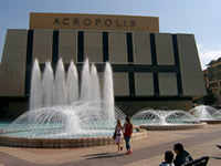
Welcome to Nice and the E-MRS/IUMRS ICEM 2006 Spring Meeting!
Bienvenue à Nice Pour le Congrès E-MRS/IUMRS ICEM- Session du Printemps 2006!
The E-MRS 2006 Spring Meeting
began in Nice, France, on Monday with most symposia commencing
sessions. The IUMRS - ICEM (International Conference on Electronic
Materials) 2006 meeting is being held in conjunction with the E-MRS
spring meeting. The thread of electronic materials and devices thus ran
through several symposia. Of the 23 technical symposia that were
organized within 6 clusters, 21 symposia started sessions on Monday. A
selection of talks from the meeting are described below giving a flavor
of the various sessions held and the range of materials research areas
covered. Several symposia included poster sessions as well.
Butterfly Scales as Living Photonic Crystals
Symposium A - Current Trends in Nanoscience
Opal is a well-known natural photonic crystal. However, there are
examples of photonic crystals in the biological world as well. Lazlo Peter Biró
(Research Inst. for Technical Physics and Materials Science, Hungary)
described the scales on the wings of butterflies that also rather
surprisingly demonstrate photonic crystal properties and give rise to
startling colors. Biró discussed two butterfly species, the Cyanophyrs Remus, found in South America, and the Albalina Metalica,
found in the Himalayas. The former shows blue color on its dorsal side
of the wings and green on the ventral side. The latter reveals a dorsal
blue and a metallic green. The wings of butterflies have a heirarchical
structure with scales (50 x 100 micrometers) that have ridges and cross
ribs (on the micrometer scale) that furthe r contain a <100 nm
nanostructure. It was discovered that it is the nanostructure that
gives rise to color.
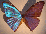
Courtesy L. P. Biró
Research Institute for Technical Physics and Material Science, Hungary
In the Cyanophyrs Remus, the blue side was found to consist of 5-10 micrometer single crystals while the green side was polycrystalline. In the Albalina Metalica
on the other hand, the colors were obtained from polycrystalline
structures though with somewhat different structures. These biological
photonic crystals were found to be very efficient reflectors and showed
amazing flexibility. It is to be noted that the colors are physical
colors and not due to pigments. Subtle differences in the structures
yielded very different colors. Biró
concluded by indicating that understanding the microstructures of these
butterflies could lead to photonic crystal materials with interesting
properties.
 |
 |
Encapsulation of Ge Nanowires in Protective Carbon Shells
Symposium E - Nanotubes and Nanowires
Germanium
nanowires are interesting for electronic applications due to quantum
size effects and due to the fact that they are compatible with existing
Si circuits. However, Ge nanowires oxidize easily which degrades their
electronic properties. Eli Sutter (Brookhaven National Lab., U.S.A.)
described the formation of carbon graphene layers on the surfaces of Ge
nanowires to prevent oxidation. She used in situ TEM
observations to study the synthesis of the nanowires. The nanowires
were grown using an Au catalyst at the tip, which was actually an
Au-rich Au-Ge material. Dark Au spots were observed on the nanowires
due to Au clusters migrating to the surface. While an oxide layer
formed immediately, it was removed by heating to 200-300°C. Ordered
C-shells, in the form of graphene sheets, were formed on the nanowires
due to the presence of the Au clusters on the surface. Thus, the
residual Au on the surface triggered the formation of protective graphe
ne layers on the surface. Sutter also indicated that the technique
could be used for other semiconductor wires.
Sensing Using Nanotubes and Nanowires
Symposium G - Functional Materials for Micro and Nanosystems
Nanowires
and nanotubes have been previously used for sensing applications using
electrically driven sensors that function by an absorbate-mediated
conductivity mechanism. Peidong Yang (Univ. California, Berkeley) and
his group however have focused on the excellent waveguiding abilities
of specific high-refractive index nanowires to create subwavelength
evanescent wave sensors that take advantage of the optical properties
of the materials. Yang demostrated waveguiding in nanowires in liquids,
including in glycol and water, that is affected by the presence of
chemicals thereby leading to sensing capabilities. He described how
such waveguides can be integrated into microfluidic devices as well
leading to applications such as detecting single DNA molecules. The
major advantage of the technique is the high sensitivity achieved as
well as the specific chemical signatures detected.
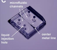
Courtesy Peidong Yang, Univ. California, Berkeley
Yang
focused the second part of his talk on single molecule detection using
inorganic nanotubes. He described results by his group on using silica
nanoparticles to detect the transport of single molecules, such as DNA
and proteins. There are two mechanisms at work. First is the actual
blockage resulting in ionic current. However, at lower concentrations
of the ionic medium such as KCl in which the device operates, there is
also DNA-induced cation enrichment that leads to an increase in the
current. Thus, there is a critical concentration between these two
conditions. Yang suggested that the use of inorganic
nanotubes/nanowires for single molecule detection represents a new
sensing platform and shows significant promise.
The Role of Defects and Texture in the Performance of Poly-Si Thin Film Transistors
Symposium I - Thin Films for Large Area Electronics
Performance
improvements in poly-Si TFTs have been spectacular after wide
acceptance of laser-based lateral crystallization technology and its
numerous variants. However, variations in TFT characteristics still
present substantial difficulties to control. In his presentation, Mark
Crowder (Sharp Labs.) presented results on a study of the
characteristics of poly-Si TFTs fabricated by laser crystallization,
and their relationship to the microstructural details of the active
layer in the TFTs. The effects of single grain boundary inclusion in
the device channel was discussed and the key causes of variation in
performance were described even in the absence of hard boundaries. The
existence of structural defects and variations in texture correlated
well with the observed variation in TFT mobility and threshold voltage.
Texture here refers to the dominant crystallographic orientation with
the region corresponding to the device active layer. The study
indicates the importance of achieving a consistent microstucture as
well as the difficulty in doing so by employing blanket crystallization
technologies.

Nanoscience Education
Symposium W - Education in Materials Science and Engineering
There
was a session on educating people in nanotechnology with three speakers
from Europe, the United States and Taiwan. Bruno Schmitz, from D.G,
European Commission, said there were several issues for the Europeans.
They need to increase the number of well-qualified researchers in
Europe to 350 million by the year 2015. The number of 350 million was
questioned by some in the audience. The obstacles to the mobility of
researchers between different geographic sectors as well as mobility
between disciplines need to be removed. A research career is not
regarded highly as a profession in Europe.
There
is a wide variation of research in Europe and the overall investment
level in commercial activities is lower than in the U. S. leading to a
problem with taking research into production and, in addition, the
coverage of patents is much lower. The question was how can E-MRS help
to maximize the impact and efficiency of European research. Funding for
research in Europe in 2004 was about the same as in the United States
at about $3B. Some of the outcomes that Europe would like to have
include developing initiatives for introducing nano-science in schools
in various languages. Also introducing nanoscience as a masters degree
while maintaining a solid discipline-based grounded education and
promoting common European Masters and PhD programs.
The speaker from the USA, Lance Haworth (National Science Foundation),
concentrated on the international activities of NSF. He said that the
fiscal 2007 request for funding (not yet appropriated) was $373M of
which $58M was dedicated to nanomaterials. Carmen Huber, who was also
the chair of the session, is responsible for international activities
in materials for NSF. Their primary goal is to enhance international
collaboration in materials research education and technology. They have
developed a Materials World Network that holds materials workshops
around the world. Since 2001, 800 proposals have led to 150 awards for
$50.2 million in partnership funded collaborations.
Yonhua
Tzeng (National Cheng Kung University, Taiwan) talked about nanoscience
developments for higher education in Taiwan. He noted that the word
“nano” in Chinese means “rice” which leads to an interesting view of
the topic. A number of companies in Taiwan use the term "nano" for
publicity (for example “Nanowater”) that Taiwan has developed a Nano
Marks System that validates the claims of manufacturers for using the
term. They have a $10M investment in advanced fabrication and
characterization facilities where 650 researchers per month conduct
state-of-the-art research and development.
© Materials Research Society, 2006 |
